Abstract
In portable device applications, host changes adapter’s output to high voltage is a general solution to achieve fast charge. This application note provides charge profile of the RT9466/RT9467 to users. Please users must to follow the charge profile to control the RT9466/RT9467 VBUS voltage.
1. Charge System Structure
The general function block of switching charge as Figure 1. The host controls VBUS voltage via PD controller or RT9466/RT9467 PE+ protocol. The gauge device provides battery capacity information to host. The RT9466/RT9467 main duty is to complete the charge cycle and provide charge status to host. The host controls the RT9466/RT9467 charge condition via I2C interface.

Figure 1. Functional Block for Switching Charger
2. Charge Profile Introduction for Low VBUS Charge Condition
The Figure 2 is charge profile for VBUS = 5V condition. Host set the VBUS to 5V by PD protocol or PE+ protocol. Users can use gauge device to determine battery charge level.
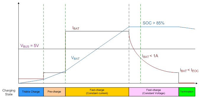
Figure 2. Charge Profile for VBUS = 5V Charge Condition
3. Charge Profile Introduction for High VBUS Charge Condition
The Figure 3 is charge profile for VBUS higher than 5V condition. In trickle charge and pre-charge period, host sets the VBUS voltage to 5V via PD or PE+ protocol. After battery enter fast charge level, host changes VBUS higher than 5V to increase charge current. After battery capacity higher than 85% and charge current lower than 1A, users must to change VBUS to 5V to finish charge cycle.
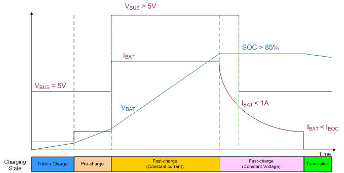
Figure 3. Charge Profile for VBUS > 5V Charge Condition